1 Global Gallium Arsenide Wafer Market Outlook
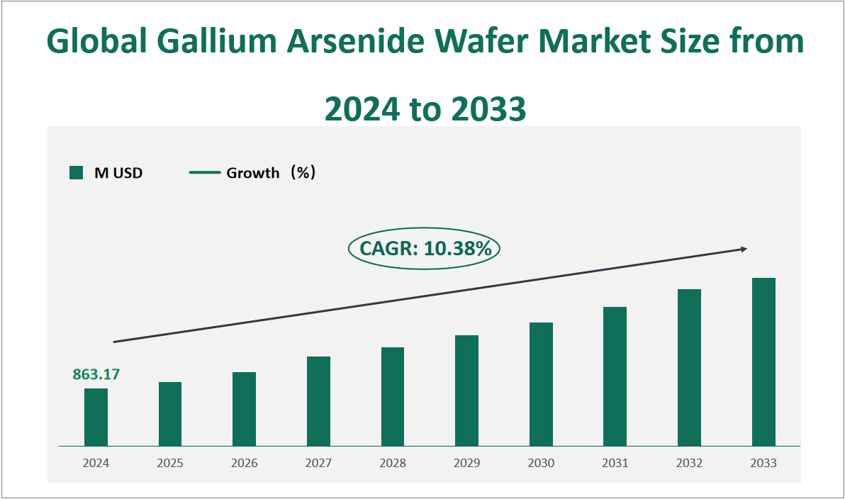
The global Gallium Arsenide Wafer market is projected to exhibit substantial growth in the coming years, with a CAGR of 10.38% from 2024 to 2033, reaching a total market size of $863.17 million USD in 2024. Gallium Arsenide (GaAs) is a compound of the elements gallium and arsenic, forming an III-V direct bandgap semiconductor with a zinc blend crystal structure. It is widely used in the manufacture of devices such as microwave frequency integrated circuits, monolithic microwave integrated circuits, infrared light-emitting diodes, laser diodes, solar cells, and optical windows. The unique electrical and optical properties of GaAs make it an essential material in various high-tech applications, from 5G communication to LED technology and photovoltaic cells.
Figure Global Gallium Arsenide Wafer Market Size and Growth Rate (2024-2033)

2 Gallium Arsenide Wafer Market Growth Drivers and Constraints
The growth of the GaAs Wafer market is driven by several key factors. Firstly, the increasing demand for high-speed and high-frequency devices in the telecommunications and electronics sectors is a significant driver. The 5G era has brought higher requirements for power, frequency, and transmission speed, making GaAs substrates ideal for RF devices. Additionally, the growing popularity of smartphones and LED technology has further expanded the application scenarios for GaAs substrates. For instance, the introduction of VCSEL for face recognition in iPhone X and the entry of major manufacturers into the Mini LED market have spurred explosive growth in demand for GaAs substrates.
However, there are also limiting factors that restrain the market’s growth. The production of GaAs wafers involves the use of arsenic, a toxic material, which poses environmental and safety challenges. Regulatory policies are continuously tightening, requiring enterprises to strengthen the management of raw materials, semi-finished products, and finished products throughout the production process. This has led to increased safety production investments to ensure legal and compliant operations. Moreover, technological updates pose a risk, as silicon on insulator (SOI) materials are making inroads in applications such as RF devices, potentially replacing GaAs wafers due to their lower cost, despite having slightly inferior performance in terms of power consumption, heat generation, and transmission speed.
3 Gallium Arsenide Wafer Market Innovations and M&A Activities
Technological innovation in the GaAs Wafer market is focused on improving manufacturing processes to enhance product quality and reduce costs. The industry is continuously refining the LEC (Liquid Encapsulated Czochralski) and VGF (Vertical Gradient Freeze) processes to produce high-quality single crystals with lower defect densities. These advancements are crucial for meeting the stringent requirements of downstream applications, especially in the fields of 5G communication and high-efficiency solar cells.
Corporate mergers and acquisitions have also played a role in shaping the market landscape. For example, Sumitomo Electric Industries, a leading player in the market, has a long history of innovation and expansion in the field of compound semiconductors. Their products, including GaAs wafers, are used in a wide range of applications, from communication terminals to automotive components. Through strategic acquisitions and partnerships, Sumitomo Electric Industries has been able to expand its market reach and enhance its product portfolio.
In conclusion, the global GaAs Wafer market is expected to grow significantly, driven by the increasing demand for high-performance semiconductor materials. However, the market must also navigate challenges related to environmental regulations and technological competition. Technological advancements and strategic corporate actions will continue to influence the market’s trajectory, shaping its future in the years to come.
4 Global Gallium Arsenide Wafer Market Analysis by Type
In 2024, the global gallium arsenide wafer market is forecasted to generate a total revenue of 863.17 million USD. The market share distribution by type is as follows: LEC Grown GaAs is expected to account for 41.45% of the total revenue, with a revenue of 357.80 million USD, while VGF Grown GaAs is projected to hold 58.55% of the market revenue, with a revenue of 505.37 million USD. This indicates that VGF Grown GaAs will continue to dominate the market in terms of revenue generation in 2024.
Table Global Gallium Arsenide Wafer Market Size and Share by Type in 2024
Type | Market Size in 2024 (M USD) | Market Share in 2024 (%) |
|---|---|---|
LEC Grown GaAs | 357.80 | 41.45% |
VGF Grown GaAs | 505.37 | 58.55% |
5 Global Gallium Arsenide Wafer Market Analysis by Application
In 2024, the global gallium arsenide wafer market is forecasted to generate a total revenue of 863.17 million USD. The market share distribution by application is as follows: RF is expected to account for 25.40% of the total revenue, LED for 52.13%, Photonics for 18.26%, and Photovoltaic for 4.21%. The specific revenue for each application is as follows: RF is forecasted to generate 219.27 million USD, LED is expected to contribute 449.89 million USD, Photonics will account for 157.65 million USD, and Photovoltaic will generate 36.36 million USD. This indicates that LED applications will continue to dominate the market in terms of revenue generation in 2024.
Table Global Gallium Arsenide Wafer Market Size and Share by Application in 2024
Application | Market Size in 2024 (M USD) | Market Share in 2024 (%) |
|---|---|---|
RF | 219.27 | 25.40% |
LED | 449.89 | 52.13% |
Photonics | 157.65 | 18.26% |
Photovoltaic | 36.36 | 4.21% |
6 Global Gallium Arsenide Wafer Market Analysis by Region
In 2024, the global gallium arsenide wafer market is forecasted to generate a total revenue of 863.17 million USD. The market share distribution by region is as follows: North America is expected to account for 13.50% of the total revenue, with a revenue of 116.57 million USD; Europe for 9.98% with a revenue of 86.16 million USD; Asia-Pacific for 75.42% with a revenue of 651.01 million USD; South America for 0.33% with a revenue of 2.84 million USD; and the Middle East and Africa for 0.76% with a revenue of 6.58 million USD. This indicates that the Asia-Pacific region will continue to dominate the market in terms of revenue generation in 2024.
Figure Global Gallium Arsenide Wafer Market Share by Region in 2024

7 Top 3 Companies of Global Gallium Arsenide Wafer Market
7.1 Sumitomo Electric Industries, Ltd.
Company Introduction and Business Overview:
Sumitomo Electric Industries, Ltd. is a leading global manufacturer of electric wires, cables, and related equipment. Established in 1897, the company is headquartered in Japan and operates worldwide. Sumitomo Electric Industries is known for its extensive product range, including optical fibers, wire harnesses, antennas for broadcasting stations, and electric monitoring systems. The company also produces disc brakes and antilock braking systems for automobiles and printed circuit boards.
Products Offered:
Sumitomo Electric Industries provides a wide range of compound semiconductors, including gallium arsenide (GaAs) and gallium nitride (GaN). These materials are used in the production of microwave frequency integrated circuits, monolithic microwave integrated circuits, infrared light-emitting diodes, laser diodes, solar cells, and optical windows. The company’s GaAs wafers are particularly noted for their high electron mobility and low defect density, making them ideal for high-frequency and high-power applications.
Sales Revenue in the Latest Year:
Sumitomo Electric Industries is expected to generate a significant portion of the global GaAs wafer market revenue. The company’s revenue from GaAs wafers is forecasted to be $225.43 million, with a market share of 29.05%. This places Sumitomo Electric Industries at the forefront of the GaAs wafer market, driven by its strong technological capabilities and global market presence.
7.2 Freiberger Compound Materials GmbH
Company Introduction and Business Overview:
Freiberger Compound Materials GmbH is a leading manufacturer of compound semiconductor substrates for microelectronics and optoelectronics. Established in 1995, the company is headquartered in Germany and has a global market distribution. Freiberger Compound Materials is known for its high-quality GaAs wafers, which are used in a variety of applications, including radio frequency (RF) devices, light-emitting diodes (LEDs), and photovoltaic cells.
Products Offered:
Freiberger Compound Materials offers a range of GaAs wafers, including those grown using the LEC (Liquid-Encapsulated Czochralsky) and VGF (Vertical Gradient Freeze) processes. The company’s wafers are characterized by their high purity, low defect density, and excellent electrical properties. These wafers are used in the production of high-performance electronic and optoelectronic devices, making them a preferred choice for many manufacturers.
Sales Revenue in the Latest Year:
Freiberger Compound Materials GmbH is expected to generate a revenue of $166.45 million from GaAs wafers, with a market share of 21.12%. The company’s strong focus on quality and innovation has helped it maintain a significant position in the global GaAs wafer market.
7.3 AXT, Inc.
Company Introduction and Business Overview:
AXT, Inc. is a leading provider of high-performance semiconductor substrates for electronic and optoelectronic applications. Established in 1986, the company is headquartered in the United States and has a global market distribution. AXT, Inc. is known for its extensive product range, including GaAs substrates with diameters ranging from 1 inch to 6 inches. The company’s substrates are used in a variety of applications, including LEDs, RF devices, and photovoltaic cells.
Products Offered:
AXT, Inc. offers a wide range of GaAs substrates, which are used in the production of high-performance electronic and optoelectronic devices. The company’s substrates are known for their high quality and consistency, making them a preferred choice for many manufacturers. AXT, Inc. also provides a range of raw materials and services to support the production of semiconductor devices.
Sales Revenue in the Latest Year:
AXT, Inc. is expected to generate a revenue of $119.88 million from GaAs wafers, with a market share of 15.29%. The company’s strong product portfolio and global market presence have helped it maintain a significant position in the GaAs wafer market.

