1 Global Thick Layer Photoresists Market Outlook
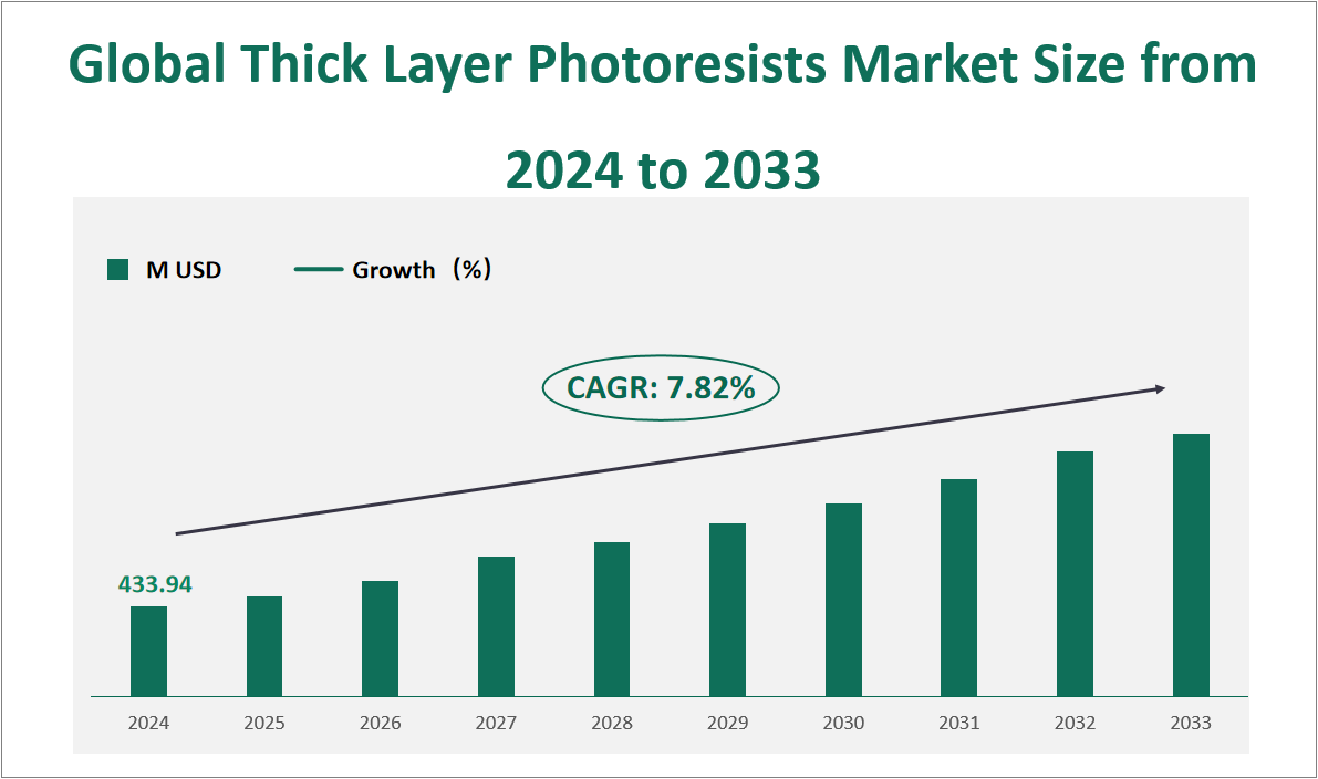
The global Thick Layer Photoresists market is projected to exhibit substantial growth in the coming years, with a CAGR of 7.82% from 2024 to 2033, reaching a total market size of $433.94 million USD in 2024. Thick Layer Photoresists are specialized materials used in photolithography processes to create high-resolution patterns on substrates. These materials are essential for manufacturing integrated circuits, microelectromechanical systems (MEMS), and other advanced electronic components. They are characterized by their ability to form thick films with high resolution and durability, making them ideal for applications such as solder bumping, copper pillar plating, and wafer-level packaging.
Figure Global Thick Layer Photoresists Market Size and Growth Rate (2024-2033)

2 Thick Layer Photoresists Market Growth Drivers and Constraints
The growth of the global Thick Layer Photoresists market is influenced by several driving factors. The primary driver is the increasing demand from the semiconductor industry, where Thick Layer Photoresists are essential for advanced packaging technologies. As the global economy continues to grow and the demand for electronic devices increases, the need for high-performance photoresists also rises. Additionally, the rise of artificial intelligence, cloud computing, and the Internet of Things (IoT) has further fueled the demand for semiconductors, thereby boosting the market for Thick Layer Photoresists.
However, the market also faces several limiting factors. One significant challenge is the high entry barriers due to the complex nature of photoresist manufacturing. The industry requires substantial capital investment and advanced R&D capabilities, making it difficult for new entrants to compete with established players. Additionally, the market is highly concentrated, with a few major companies controlling the majority of the market share. This concentration can limit competition and innovation, potentially hindering market growth.
Another limiting factor is the impact of global economic conditions and geopolitical events. For example, natural disasters, such as earthquakes, can disrupt production lines, as seen in Japan, where local production was affected, leading to supply shortages. The COVID-19 pandemic also had a significant impact on the industry, causing delays in production and supply chains. These disruptions highlight the vulnerability of the market to external shocks.
3 Thick Layer Photoresists Market Innovations and M&A Activities
Technological innovation plays a crucial role in the Thick Layer Photoresists market. Companies are continuously investing in R&D to develop new formulations and improve existing products. For example, JSR Corporation has been actively involved in acquiring innovative companies to enhance its technology portfolio. In 2021, JSR acquired Inpria Corporation, a leading innovator in metal oxide photoresist design, to strengthen its position in extreme ultraviolet (EUV) lithography. This acquisition highlights the importance of strategic partnerships and mergers in driving technological advancements.
Corporate mergers and acquisitions are also shaping the market landscape. Major players are leveraging these strategic moves to expand their product offerings and enhance their market presence. For instance, Merck KGaA’s acquisition of AZ Electronic Materials in 2014 significantly bolstered its capabilities in the photoresist market. These acquisitions not only provide companies with new technologies but also strengthen their market positions by integrating complementary product lines.
In addition to technological advancements, the market is also influenced by macroeconomic factors and industry trends. The increasing demand for high-performance semiconductors and the growth of emerging technologies such as 5G and artificial intelligence are driving the need for more sophisticated photoresist materials. Companies that can adapt to these trends and innovate quickly will be well-positioned to capture a larger share of the market.
In conclusion, the global Thick Layer Photoresists market is poised for significant growth, driven by the increasing demand from the semiconductor industry and advancements in technology. While challenges such as high entry barriers and economic uncertainties exist, companies that focus on innovation and strategic partnerships will be best positioned to succeed in this dynamic market.
4 Global Thick Layer Photoresists Market Analysis by Type
In 2024, the global Thick Layer Photoresists market is projected to have a total sales volume of 7,289.8 thousand liters. The market is segmented by application into Circuit Board Wiring, Micro Bump, Flip Chip Bump, MEMS, and Electrodeposition. Specifically, Circuit Board Wiring is expected to account for 2,201.8 thousand liters of sales, representing 30.20% of the total market share. Micro Bump is projected to reach 1,355.8 thousand liters, holding 18.60% of the market share. Flip Chip Bump is anticipated to have sales of 1,536.9 thousand liters, making up 21.08% of the market. MEMS is expected to contribute 1,251.3 thousand liters, accounting for 17.17% of the market share, while Electrodeposition is projected to reach 943.9 thousand liters, representing 12.95% of the market.
Table Global Thick Layer Photoresists Sales and Share by Type in 2024
Type | Sales in 2024 (K Liters) | Market Share in 2024 (%) |
|---|---|---|
Positive Polarity | 3206.0 | 43.98% |
Negative Polarity | 4083.8 | 56.02% |
5 Global Thick Layer Photoresists Market Analysis by Application
In 2024, the global Thick Layer Photoresists market is projected to have a total sales volume of 7,289.8 thousand liters. The market is segmented by application into Circuit Board Wiring, Micro Bump, Flip Chip Bump, MEMS, and Electrodeposition. Specifically, Circuit Board Wiring is expected to account for 2,201.8 thousand liters of sales, representing 30.20% of the total market share. Micro Bump is projected to reach 1,355.8 thousand liters, holding 18.60% of the market share. Flip Chip Bump is anticipated to have sales of 1,536.9 thousand liters, making up 21.08% of the market. MEMS is expected to contribute 1,251.3 thousand liters, accounting for 17.17% of the market share, while Electrodeposition is projected to reach 943.9 thousand liters, representing 12.95% of the market.
Table Global Thick Layer Photoresists Sales and Share by Application in 2024
Application | Sales in 2024 (K Liters) | Market Share in 2024 (%) |
|---|---|---|
Circuit Board Wiring | 2201.8 | 30.20% |
Micro Bump | 1355.8 | 18.60% |
Flip Chip Bump | 1536.9 | 21.08% |
MEMS | 1251.3 | 17.17% |
Electrodeposition | 943.9 | 12.95% |
6 Global Thick Layer Photoresists Market Analysis by Region
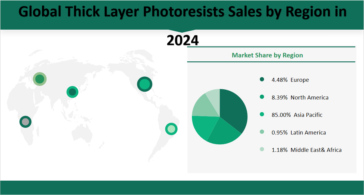
In 2024, the global Thick Layer Photoresists market is projected to reach a total sales volume of 7,289.8 thousand liters. Regionally, Asia-Pacific is expected to dominate with 6,196.1 thousand liters of sales, representing 85.00% of the global market share. Europe is anticipated to have 326.8 thousand liters of sales, holding 4.48% of the market. North America is projected to account for 611.5 thousand liters, making up 8.39% of the market. Latin America is expected to contribute 69.6 thousand liters, representing 0.95% of the market share, while the Middle East & Africa is projected to have 85.7 thousand liters of sales, accounting for 1.18% of the global market.
Figure Global Thick Layer Photoresists Sales Market Share by Region in 2024

7 Top 3 Companies of Global Thick Layer Photoresists Market
7.1 JSR Corporation
Company Introduction and Business Overview:
JSR Corporation is a leading global provider of advanced materials for the semiconductor and electronics industries. Established in 1957, JSR operates through four main business segments: elastomers, plastics, digital solutions, and life sciences. The company’s digital solutions segment is particularly notable for its offerings in photoresist materials, which are essential for semiconductor manufacturing. JSR has a strong global presence with manufacturing facilities primarily located in Japan and sales networks spanning across the United States, Europe, China, South Korea, Taiwan, and Thailand.
Products Offered:
JSR Corporation offers a comprehensive range of Thick Layer Photoresists, including the ELPAC™ THB Series. These products are designed for high-resolution applications such as wiring formation on circuit boards, micro bumps, and flip chip bumps. The ELPAC™ series is known for its excellent resolution, resistance to various plating liquids, and durability in vacuum processes. JSR’s photoresists are capable of achieving film thicknesses ranging from 10 to 100 microns, making them suitable for a wide range of applications in semiconductor packaging and MEMS manufacturing.
Sales Revenue in the Latest Year:
JSR Corporation’s Thick Layer Photoresists segment generated a revenue of $87.09 million USD. This revenue is supported by the company’s strong market position and continuous investment in R&D to develop innovative solutions for the evolving semiconductor industry.
7.2 TOK
Company Introduction and Business Overview:
TOKYO OHKA KOGYO CO., LTD (TOK) is a prominent material manufacturing company specializing in photoresists and high-purity chemicals for semiconductor and display photolithography processes. Established in 1940, TOK operates through two main business segments: materials and equipment. The company’s headquarters are in Japan, and it has a significant presence in Asia-Pacific, North America, and Europe. TOK’s materials segment is particularly strong in providing photoresist products that meet the stringent requirements of semiconductor and display manufacturing.
Products Offered:
TOK offers a wide range of Thick Layer Photoresists tailored for various applications in semiconductor packaging and MEMS manufacturing. Their product portfolio includes photoresists for copper, nickel, tin, silver, and palladium plating, which are essential for forming microbumps, gold stud bumps, and copper posts in advanced packaging technologies. TOK’s photoresists are known for their high sensitivity, high resolution, and excellent plating resistance, making them ideal for applications such as 3D through-silicon-via (TSV) and wafer-level chip-scale packages (WLCSP).
Sales Revenue in the Latest Year:
TOK’s Thick Layer Photoresists segment achieved a revenue of $72.51 million USD. This revenue reflects the company’s strong market position and its ability to provide high-quality photoresist solutions that meet the evolving needs of the semiconductor industry.
7.3 Dow Inc.
Company Introduction and Business Overview:
Dow Inc. is a global leader in materials science, committed to delivering innovative and sustainable solutions for a variety of industries, including packaging, infrastructure, and consumer care. Established in 1802, Dow operates through several business segments, including Performance Plastics, Performance Chemicals, Agricultural Sciences, and Electronic & Specialty Materials. Dow’s Electronic & Specialty Materials segment is particularly notable for its offerings in photoresist products, which cater to the needs of the semiconductor industry.
Products Offered:
Dow Inc. offers a robust lineup of Thick Layer Photoresists, including the SHIPLEY BPR™-100 Photoresist. This product is designed for use in a wide range of plating and etching processes in Wafer Level Packaging (WLP) manufacturing. SHIPLEY BPR™-100 is capable of achieving single-spin film thicknesses greater than 100 microns, making it suitable for applications such as copper pillar and flip chip packaging. The photoresist is known for its excellent adhesion to various substrates, including aluminum, copper, gold, nickel, titanium, chromium, silicon, silicon oxide, glass, ceramic, and polyamide.
Sales Revenue in the Latest Year:
Dow Inc.’s Thick Layer Photoresists segment generated a revenue of $66.34 million USD. This revenue is supported by Dow’s extensive product portfolio and its commitment to continuous innovation and sustainability in materials science.

