1 Global Mask Blank Market Insight Analysis
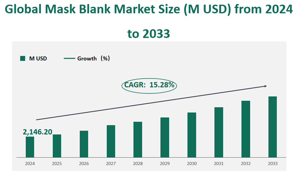
The global Mask Blank market size is expected to be USD 2,146.20 million in 2024, with a CAGR of 15.28% from 2024 to 2033.
Mask Blank is a core part of a photomask used in the semiconductor lithography process. As semiconductor technology develops, a high-definition photomask is required to form delicate patterns, along with a blank mask that can support it. Mask Blank is a glass substrate to be used as a material for making photomasks.
From these Mask Blanks, Masks are produced that are used in the photolithography production of semiconductor integrated circuits and form ultra-fine patterns with 40-nanometer width and below. Mask Blanks are the products formed from chrome or molybdenum silicide-based thin film on main quartz or soda-lime glass substrate. And they are coated by photosensitive resist materials which are sensitive to electron or laser beams and resist for the etching process to make circuit patterns.
Figure Global Mask Blank Market Size (M USD) and CAGR (2024-2033)

2 Mask Blank Market Growth Drivers and Restraints
Development of the semiconductor and electronics industry: Semiconductors are the core of electronic devices, and their market growth is due to the rising demand for global consumer electronic devices. The rise of technologies such as artificial intelligence, the Internet of Things, and machine learning has created new opportunities for the semiconductor market, promoted the production of efficient photomasks, and increased the demand for mask substrates.
As semiconductor manufacturers actively expand their production capacity, the demand for nanoscale chips continues to grow. As a key material in semiconductor lithography, the market demand for mask substrates has also risen. Driven by the development of 5G communication technology, the demand for high-performance semiconductors has surged, driving the production of related chips and expanding the market size of mask substrates.
Driven by technological innovation: The acceleration of technological innovation has led to a growing demand for high-functional materials and components. In the field of flat panel displays, as products develop towards larger screen sizes, the requirements for mask plate accuracy are also getting higher and higher.
The advancement of integrated circuit technology has promoted the development of semiconductor circuit patterns towards high miniaturization, and has put forward higher requirements for the key dimensional accuracy, registration accuracy control, and defect control of mask plates. EUV lithography, as a cutting-edge miniaturization technology, has received widespread attention. Its development is expected to further improve the precision and efficiency of chip manufacturing, thereby increasing the demand for EUV mask substrates.
Mask substrate defect problem: In EUV lithography, mask substrate defects are a major challenge. EUV mask substrates are composed of multi-layer complex structures. During the manufacturing process, defects may occur in various links such as substrates, multi-layer blank layers, and absorber patterning. These defects will affect the manufacturing yield of chips and increase production costs. Although some progress has been made in defect detection, mode conversion, and defect repair, the relevant equipment is still immature and expensive, and there are many deficiencies in practical applications, which restricts the further development of the industry.
High production cost: The production cost of mask substrates is high, which is mainly caused by a variety of factors. On the one hand, the prices of its raw materials such as glass substrates and photoresists fluctuate greatly, and some high-precision raw materials rely on imports, and the supply is relatively concentrated, making it difficult to control the cost of raw materials. On the other hand, the mask substrate industry is a technology-intensive and capital-intensive industry.
Most of the production equipment relies on imports, the equipment procurement cost is high, and the global annual equipment output is limited, and the procurement competition is fierce. In addition, the long talent training cycle also increases the cost pressure of enterprises. In the market competition, it is difficult for manufacturers to fully pass on the cost increase to customers, which has an adverse impact on the profit margins and market competitiveness of enterprises, thus restricting the growth of the market.
3 Technological Innovations in the Mask Blank Market
Breakthrough in lithography technology: In the field of semiconductor manufacturing, innovation in lithography technology is a key force driving the development of the industry. EUV lithography technology has become the focus, which can achieve finer chip patterning and meet the needs of semiconductors to continue to develop towards high performance and high integration. For example, Samsung Electronics plans to use EUV lithography technology for 3nm process semiconductor production lines, which puts higher requirements on the quality and performance of EUV mask substrates.
Relevant companies such as AGC have actively invested in research and development. The EUV mask substrates they developed have excellent flatness and extremely low defect rates. They have also cooperated with Sematech to develop the next-generation cover film process, which improves the durability of the product and provides strong support for the widespread application of EUV lithography technology.
Material innovation: In order to improve the performance of mask substrates, material innovation is crucial. Studies have found that diamond-like carbon may become a new covering material for EUV mask substrates. This discovery provides a new direction for improving the quality and stability of mask substrates. Applied conducted research on the backside materials of EUV mask substrates and proposed using harder materials to reduce defects. The chromium nitride variant developed by Applied has a higher critical load and is expected to be used in the next generation of mask substrates, which has promoted the advancement of industry technology.
AGC’s capacity expansion: As an important company in the industry, AGC decided to expand its production capacity for EUV lithography mask substrates in order to meet the growing demand for EUV lithography mask substrates for future high-performance semiconductor production. This move is based on an accurate judgment of market trends. By increasing production capacity, AGC can consolidate its position in the market and increase its market share.
The project has been supported by the Ministry of Economy, Trade and Industry of Japan and has been included in the “Promoting Japanese Investment to Strengthen the Supply Chain Plan”, which reflects the government’s attention to the semiconductor materials industry and AGC’s leading role in the industry.
S&S Tech’s equipment upgrade: S&S Tech plans to install key equipment to manufacture EUV blank masks, which shows that the company actively follows the industry’s technology development trends and strives to improve its competitiveness in the high-end mask substrate market. The installation of the ion beam deposition (IBD) machine from Veeco Instruments of the United States will help S&S Tech accumulate relevant technologies and achieve the transition from traditional mask substrate production to EUV mask substrate production, open up new market space for the company, and intensify competition in the high-end product market within the industry.
4 Global Mask Blank Market Size by Type
Low Reflectance Chrome-film Mask Blanks are the most widely used type of mask blanks in the industry. These blanks are known for their high durability, opacity, and adhesion properties, making them ideal for a wide range of semiconductor manufacturing processes. In 2024, the revenue generated from Low Reflectance Chrome-film Mask Blanks is projected to reach $1,203.59 million. This type is expected to hold a significant market share of 56.08% in the global mask blank market.
The growth of this segment is driven by the increasing demand for high-resolution photomasks, particularly in the production of advanced semiconductor chips. These blanks are essential for creating ultra-fine patterns with widths below 40 nanometers, which are critical for the performance of modern electronics. The market share of Low Reflectance Chrome-film Mask Blanks is expected to remain dominant due to their versatility and reliability in various applications.
Attenuated Phase Shift Mask Blanks represent a more specialized segment of the mask blank market. These blanks are designed to improve image resolution in lithography by using phase differences to enhance pattern clarity. In 2024, the revenue from Attenuated Phase Shift Mask Blanks is forecasted to be $942.61 million, accounting for a market share of 43.92%.
The demand for Attenuated Phase Shift Mask Blanks is driven by the need for higher precision and integration in semiconductor manufacturing. These blanks are particularly useful in the production of advanced logic and memory chips, where high-density patterns are required. The market share of this type is expected to grow steadily as the industry moves towards more advanced lithography techniques, such as Extreme Ultraviolet (EUV) lithography.
Table Global Mask Blank Market Size and Share by Type in 2024
|
Type |
Market Size (M USD) 2024 |
Market Share 2024 |
|---|---|---|
|
Low Reflectance Chrome-film Mask Blanks |
1203.59 |
56.08% |
|
Attenuated Phase Shift Mask Blanks |
942.61 |
43.92% |
5 Global Mask Blank Market Size by Application
In terms of market revenue, the semiconductor application takes the lead. According to the data, the market revenue for semiconductor – related mask blanks in 2024 is projected to reach 1333.68 million USD. This significant figure underscores the crucial role of mask blanks in semiconductor manufacturing. Semiconductors are the backbone of modern electronics, powering everything from smartphones to data centers. The continuous miniaturization and performance enhancement requirements in semiconductor technology drive the high demand for mask blanks.
Following semiconductors is the flat panel display application, with a market revenue of 527.19 million USD in 2024. The growth of the flat panel display industry, fueled by the increasing demand for larger and higher – resolution displays in televisions, computer monitors, and mobile devices, has contributed to this revenue. Mask blanks are essential in the lithography processes used to create the intricate patterns on flat panel displays.
The touch industry also contributes to the mask blank market, with a revenue of 83.05 million USD in 2024. As touch – enabled devices such as smartphones, tablets, and touch – screen kiosks become more prevalent, the need for mask blanks in the production of touch sensors and related components grows.
The circuit board application has a market revenue of 81.40 million USD in 2024. Circuit boards are fundamental components in all electronic devices, and the mask blanks are used in the manufacturing process to create precise circuitry patterns.
Table Global Mask Blank Market Size and Share by Application in 2024
|
Application |
Market Size (M USD) 2024 |
Market Share 2024 |
|---|---|---|
|
Semiconductor |
1333.68 |
62.14% |
|
Flat Panel Display |
527.19 |
24.56% |
|
Touch Industry |
83.05 |
3.87% |
|
Circuit Board |
81.40 |
3.79% |
|
Others |
120.88 |
5.63% |
6 Global Mask Blank Market Size by Region
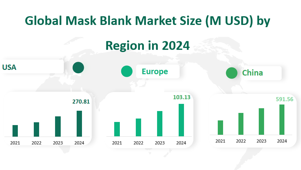
The United States is projected to be a substantial market for mask blanks in 2024, with an estimated revenue of $270.81 million. This significant figure reflects the U.S.’s robust semiconductor industry, which is a leader in innovation and technology. The growth in the U.S. can be attributed to the country’s focus on advancing semiconductor technologies, including investments in research and development, as well as the presence of major semiconductor manufacturers. The U.S. market is also supported by a strong ecosystem of suppliers and a skilled workforce, which are essential for the production of high-quality mask blanks.
Europe is expected to contribute $103.13 million to the global mask blank market in 2024. The European market is characterized by a strong emphasis on technological advancement and sustainability. European countries are investing heavily in semiconductor manufacturing capabilities, driven by the need for self-sufficiency in critical technologies and the push towards digital transformation across various industries. The region’s commitment to innovation is further bolstered by collaborative efforts among European nations to develop advanced semiconductor technologies, which includes the production of mask blanks.
China stands out as a rapidly growing market, with an impressive revenue projection of $591.56 million for 2024. The Chinese market’s growth is fueled by the country’s aggressive expansion in the semiconductor sector. China’s strategic investments in domestic semiconductor manufacturing capabilities aim to reduce reliance on imports and boost its position in the global technology supply chain. The government’s support for the industry, along with favorable policies and funding, has led to a surge in the establishment of new facilities and the upgrading of existing ones. This has created a substantial demand for mask blanks, driving the market’s revenue in China.
Figure Global Mask Blank Market Size (M USD) by Region in 2024

7 Global Mask Blank Market Analysis by Major Players
HOYA Corporation
Company Profile: HOYA Corporation, headquartered in Japan, is a leading global med-tech company established in 1941. It operates worldwide, offering a diverse range of high-tech and medical products.
Business Overview: HOYA is active in healthcare and information technology, providing eyeglasses, medical endoscopes, intraocular lenses, optical lenses, and key components for semiconductor devices, LCD panels, and HDDs. With over 160 offices and subsidiaries globally, HOYA employs approximately 38,000 people.
Product Offered: HOYA leads in the development of products for EUV lithography, offering mask blanks and photomasks essential for semiconductor manufacturing.
2023 Financial Summary: In 2023, HOYA achieved a revenue of $802.90 million with a gross margin of 37.80%, reflecting its strong market position and financial health.
Shin-Etsu MicroSi, Inc.
Company Profile: Shin-Etsu MicroSi, Inc., a U.S. subsidiary of Shin-Etsu Chemical, was established in 1989 and is headquartered in Japan. It operates globally, focusing on semiconductor and coating industries.
Business Overview: Shin-Etsu MicroSi, Inc. specializes in research, development, and manufacturing of materials for semiconductor and coating industries, providing high-performance products designed for photolithography, packaging, solar, and flexible printed circuit requirements.
Product Offered: The company supplies photomask blanks, including attenuated phase-shift photomask blanks for ArF and KrF, which are crucial for advanced semiconductor manufacturing processes.
2023 Financial Summary: Shin-Etsu MicroSi, Inc. reported a revenue of $572.33 million and a gross margin of 37.53% in 2023, indicating its profitability and market competitiveness.
AGC Inc.
Company Profile: AGC Inc., established in 1997 and headquartered in Japan, is a global leader in glass, chemicals, and high-tech materials, with a worldwide sales reach.
Business Overview: AGC Electronics America, a division of AGC Flat Glass North America, manufactures materials for the semiconductor industry and distributes other AGC Electronics Materials. AGC is a market leader in automotive and building glass, with operations in over 30 countries.
Product Offered: AGC offers extreme ultraviolet lithography (EUV) mask blanks, which are essential for producing high-performance semiconductors. They have developed a proprietary next-generation capping film process for these blanks.
2023 Financial Summary: AGC Inc. generated a revenue of $289.16 million and maintained a gross margin of 36.01% in 2023, showcasing its financial stability and market influence.

